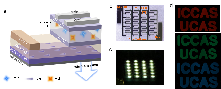
Organic light-emitting transistors (OLETs) are a novel type of optoelectronic integrated device that combines the advantages of low energy consumption and high integration. This device effectively integrates the light-emitting display function of organic light-emitting diodes (OLEDs) and the current regulation function of organic field-effect transistors (OFETs) . Therefore, compared to OLEDs, OLETs exhibit higher current regulation capability and luminous efficiency, enabling more precise pixel control. At the same time, their unique structural design endows the device with great potential in flexible displays and low-power applications, showing broad application prospects and research value in cutting-edge fields such as novel displays, optical communication, and optical diagnosis and treatment
However...
Existing white OLETs face challenges such as complex doping systems, low external quantum efficiency (EQE), and poor color purity.
Therefore we decided to address the problem!
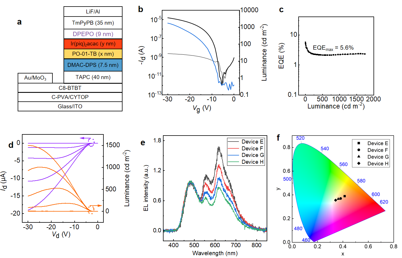
In order to improve the purity of the white liht emitted, we designed a thin-layer OLET to enhance the white light emitted. By combining the 3 organic pigments as shown below and adjusting them, we are able to create and improve the relative whiteness and purity of the light emitted.
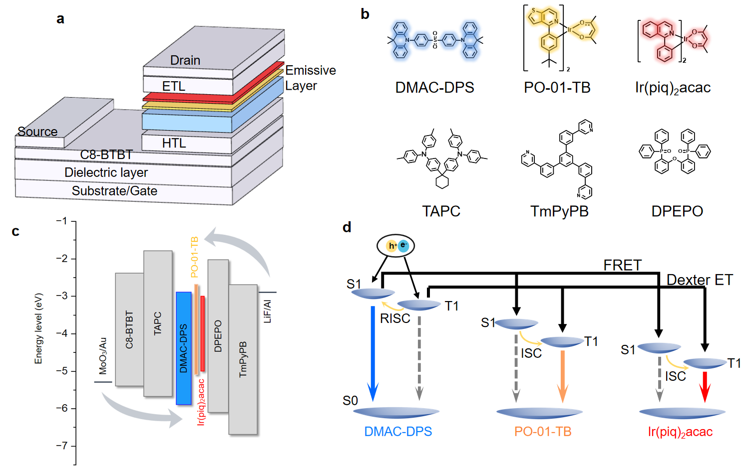
The graph showing the composition and the light-principle of the OLET
Creating the device
The device is placed on the ITO glass base.
First, the ITO glass was ultrasonically cleaned with n-hexane, chloroform, and isopropanol solvents for 10 minutes, then dried using a nitrogen gun, and finally vacuum treated with oxygen plasma (40 W) for 5 minutes.
Subsequently, the ITO glass was transferred to a glove box for the following processing steps. C-PVA (4200 r.p.m. × 45 s, annealed at 100°C for 90 minutes) / CYTOP (5000 r.p.m. × 60 s, annealed at 100°C for 30 minutes) were sequentially spin-coated on the cleaned ITO glass substrate as a dual dielectric layer.
In a vacuum chamber with a pressure of 5 × 10⁻⁶ Torr, 50 nm of C8-BTBT (0.3~0.5 Å s-1) was deposited on the glass/ITO/C-PVA/CYTOP. After replacing the mask plate, 2 nm MoO3 (0.1 Å s-1) / 40 nm Au (0.1 Å s-1) were evaporated on the C8-BTBT as the source electrode.
Then, the mask plate was replaced, and 40 nm TAPC (1 Å s-1) was deposited as a charge transport buffer layer to achieve uniform surface light source, followed by 7.5 nm DMAC-DPS (0.5 Å s-1) and 0.5 nm PO-01-TB (0.05 Å s-1) as the light-emitting layer, and 9 nm DPEPO and 35 nm TmPyPB (1 Å s-1) were deposited as the electron transport layer.
Finally, after replacing the mask plate, 2 nm LiF/110 nm Al was deposited as the drain electrode, completing the fabrication of the OLET device。
Investigation and Results
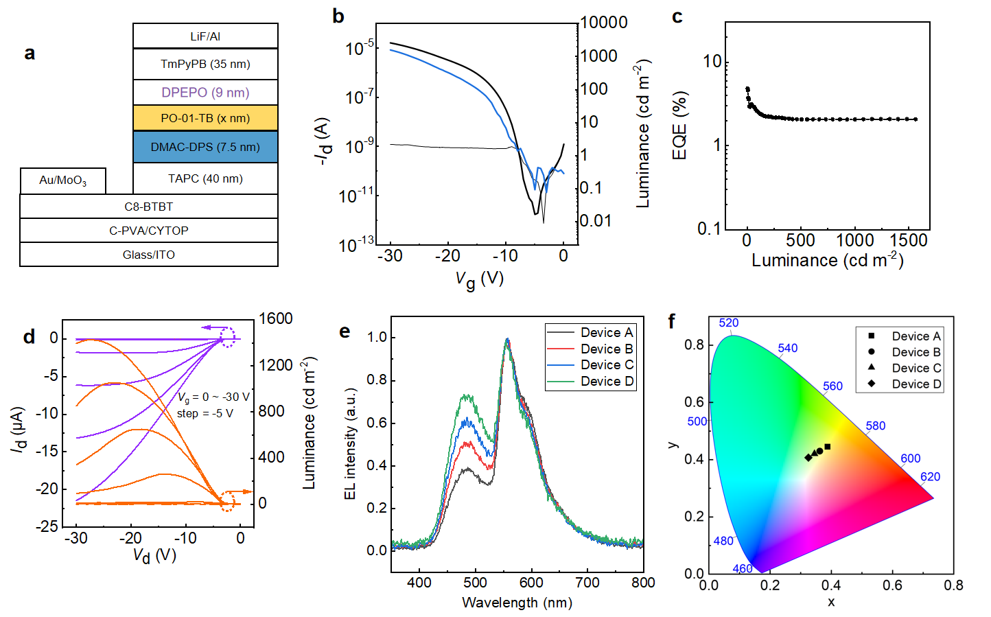
This graph shows the combination of blue and yellow light-emitting layer.
However, due to the loss of red light, the light purity results are not close and presents a significantly higher energy cost.
So for improvements,